- 您现在的位置:买卖IC网 > Sheet目录1992 > CY28317PVXC-2 (Silicon Laboratories Inc)IC CLK FTG VIA PL/E133T 48SSOP
CY28317-2
..................... Document #: 38-07094 Rev. *B Page 17 of 20
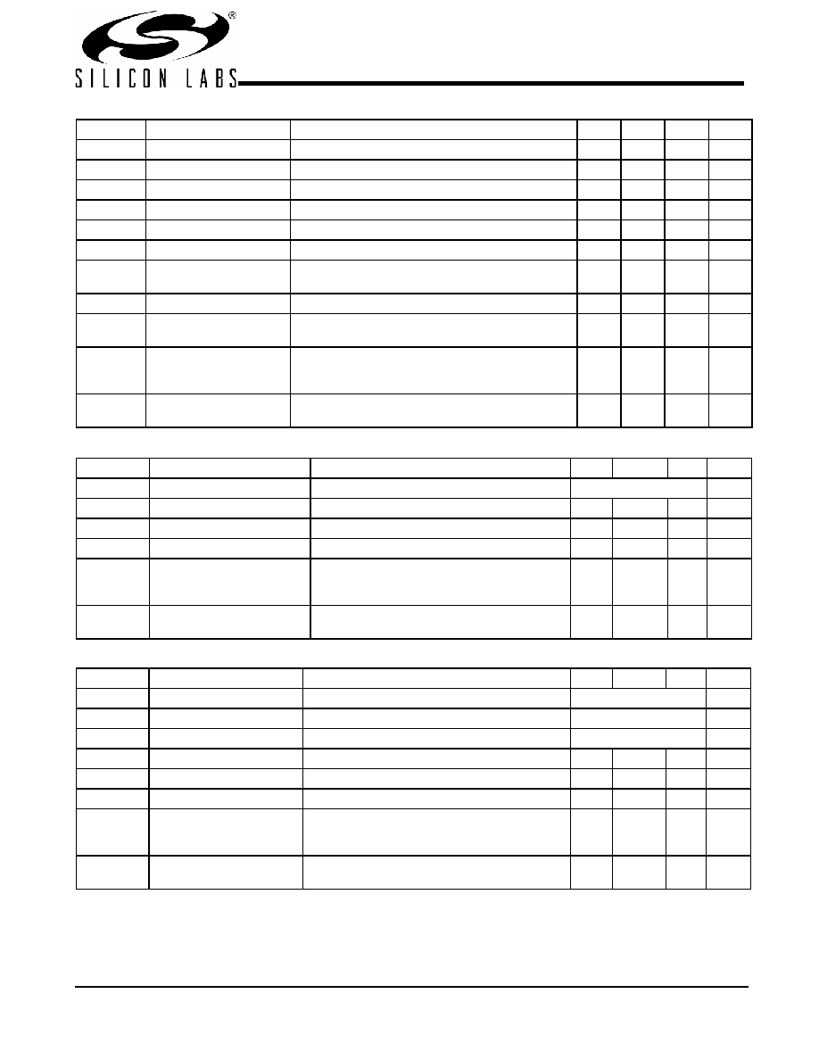
PCI Clock Outputs, PCI (Lump Capacitance Test Load = 20 pF)
Parameter
Description
Test Condition/Comments
Min.
Typ.
Max.
Unit
tP
Period
Measured on the rising edge at 1.5V
30
ns
tH
High Time
Duration of clock cycle above 2.4V
12
ns
tL
Low Time
Duration of clock cycle below 0.4V
12
ns
tR
Output Rise Edge Rate
Measured from 0.4V to 2.4V
1
4
V/ns
tF
Output Fall Edge Rate
Measured from 2.4V to 0.4V
1
4
V/ns
tD
Duty Cycle
Measured on the rising and falling edges at 1.5V
45
55
%
tJC
Jitter, Cycle-to-Cycle
Measured on the rising edge at 1.5V. Maximum
difference of cycle time between two adjacent cycles.
250
ps
tSK
Output Skew
Measured on the rising edge at 1.5V
500
ps
tO
CPU to PCI Clock Skew
Covers all CPU/PCI outputs. Measured on the rising
edge at 1.5V. CPU leads PCI output.
1.5
4
ns
fST
Frequency Stabilization
from Power-up (cold
start)
Assumes full supply voltage reached within 1 ms
from power-up. Short cycles exist prior to frequency
stabilization.
3ms
Zo
AC Output Impedance
Average value during switching transition. Used for
determining series termination value.
30
REF Clock Outputs (Lump Capacitance Test Load = 20 pF)
Parameter
Description
Test Condition/Comments
Min.
Typ.
Max.
Unit
f
Frequency, Actual
Frequency generated by crystal oscillator
14.318
MHz
tR
Output Rise Edge Rate
Measured from 0.4V to 2.4V
0.5
2
V/ns
tF
Output Fall Edge Rate
Measured from 2.4V to 0.4V
0.5
2
V/ns
tD
Duty Cycle
Measured on the rising and falling edges at 1.5V
45
55
%
fST
Frequency Stabilization from
Power-up (cold start)
Assumes full supply voltage reached within
1 ms from power-up. Short cycles exist prior to
frequency stabilization.
3ms
Zo
AC Output Impedance
Average value during switching transition. Used
for determining series termination value.
40
48-MHz Clock Output (Lump Capacitance Test Load = 20 pF)
Parameter
Description
Test Condition/Comments
Min.
Typ.
Max.
Unit
f
Frequency, Actual
Determined by PLL divider ratio (see m/n below)
48.008
MHz
fD
Deviation from 48 MHz
(48.008 – 48)/48
+167
ppm
m/n
PLL Ratio
(14.31818 MHz x 57/17 = 48.008 MHz)
57/17
tR
Output Rise Edge Rate
Measured from 0.4V to 2.4V
0.5
2
V/ns
tF
Output Fall Edge Rate
Measured from 2.4V to 0.4V
0.5
2
V/ns
tD
Duty Cycle
Measured on the rising and falling edges at 1.5V
45
55
%
fST
Frequency Stabilization
from Power-up (cold start)
Assumes full supply voltage reached within 1 ms
from power-up. Short cycles exist prior to
frequency stabilization.
3ms
Zo
AC Output Impedance
Average value during switching transition. Used
for determining series termination value.
40
发布紧急采购,3分钟左右您将得到回复。
相关PDF资料
CY28323OXC
IC CLOCK BROOKDALE GPENT4 48SSOP
CY28354OXC-400
IC BUFF 273MHZ 4DDR DIMM 48SSOP
CY28378OXC
IC CLOCK CK408/TITAN 845 48SSOP
CY284108ZXC
IC CLOCK SERV CK410B 56TSSOP
CY28410OXC-2
IC CLOCK CK410 GRANTSDALE 56SSOP
CY28410OXC
IC CLOCK CK410 GRANTSDALE 56SSOP
CY28411ZXC
IC CLOCK CK410M ALVISO 56TSSOP
CY28442ZXC-2
IC CLOCK ALVISO PENTM 56TSSOP
相关代理商/技术参数
CY28317PVXC-2T
功能描述:时钟发生器及支持产品 NB Clk VIA SDRAM Chipsets / Tualatin RoHS:否 制造商:Silicon Labs 类型:Clock Generators 最大输入频率:14.318 MHz 最大输出频率:166 MHz 输出端数量:16 占空比 - 最大:55 % 工作电源电压:3.3 V 工作电源电流:1 mA 最大工作温度:+ 85 C 安装风格:SMD/SMT 封装 / 箱体:QFN-56
CY28317ZC-2
制造商:CYPRESS 制造商全称:Cypress Semiconductor 功能描述:FTG for Mobile VIA PL133T and PLE133T Chipsets
CY28317ZC-2T
制造商:CYPRESS 制造商全称:Cypress Semiconductor 功能描述:FTG for Mobile VIA PL133T and PLE133T Chipsets
CY28322
制造商:未知厂家 制造商全称:未知厂家 功能描述:Clocks and Buffers
CY28322-2
制造商:CYPRESS 制造商全称:Cypress Semiconductor 功能描述:133-MHz Spread Spectrum Clock Synthesizer with Differential CPU Outputs
CY28322ZC-2
制造商:Rochester Electronics LLC 功能描述:- Bulk
CY28322ZC-2T
制造商:Rochester Electronics LLC 功能描述:- Bulk
CY28323
制造商:CYPRESS 制造商全称:Cypress Semiconductor 功能描述:FTG for Intel㈢ Pentium㈢ 4 CPU and Chipsets